THE DEVELOPMENT THE AUTOMATIC ACCIDENT ALERT WITH VEHICLE TRACKING SYSTEM USING GSM

Monday 6 May 2013

WEEK 14 (FYP 2)

TITTLE : PRESENTATION DAY


Finally, the day that I are waiting for. It's the day that of presentation and the most important is the competition day. Presentation about the project was held in the morning from 9.00 am until 1.00 pm, and the competition is being held in the afternoon which start at 2.30 pm until 5.00 pm. During the presentation time, I and my other friends had been assess by two assessor:-

~ Mdm Nurul Rodziah Bt. Abdul Ghafar
~ Dr Hafiz Bin Hamzah

Presentation time run smoothly without any difficulty. Picture below is my Poster of Automatic Accident Alert System.

Figure 1 : Poster of my project

Figure 2 : Show of my project

At the afternoon, the competition begin. I was very upset during the competition time. It is because, I was not selected in the top 20 project listed. Maybe all the competitor are great and tough, that why I not nominated in the top 20 I think. ='(
copyright by
sh mohd faiz

Thursday 18 April 2013

WEEK 13 (FYP 2)

TITTLE : DESIGN THE PROTOTYPE

The Last week before the Presentation and this project not finish yet. So, this week, I prepared the prototype for the project. The prototype is compulsory to all Final Year Project's student. Picture below is the example of the prototype that I've already design.


Figure 1 : Front side of the prototype


Figure 2 : Left side of the prototype


Figure 3 : Upper side of the prototype


copyright by
sh mohd faiz

Wednesday 10 April 2013

WEEK 12 (FYP 2)

TITTLE : PROGRAM PROCESS


This is the MPLAB software is very important to use or doing simulation. It related each other. To do simulation for circuit and programming, I use proteus software. For command or programming we use MPLAB software ant to burn into pic we use software pic kit. And the picture below show the result of my program Automatic Accident Alert System.


Picture below show the demonstrate how to burn the IC of PIC 16877A program into the PIC burner. Below is the step :-

1) Now WinPic800 is ready to program the PIC. This programmer is able to detect the PIC. By clicking the icon shown, the programmer will detect the type of PIC on the programmer.


2) To write Hex code to PIC we must first open the hex file. By clicking the icon shown, a browse window will appear, open the hex file by clicking the file.


3) Program the file to PIC by clicking the icon shown.


4) A confirmation window will appear, click Yes to proceed programming PIC.


5) When it is completed, the window will show the status. Click Accept and the PIC is ready to be plug out.


6) To disconnect UP00A, simply plug the USB out. No extra configuration or setting needed. Same applied when plug-in for the 2nd time, installation of driver is not required. 


copyright by
sh mohd faiz


Sunday 7 April 2013

WEEK 11 (FYP 2)

TITTLE : PROGRAM PROCESS

Below is the guide to create a program using MPLAB software.


1) Before we start, create a new folder in your c drive and rename the folder accordance to your project name/title as shown below. This folder is now become your project folder.


2) Copy the given ASM code from your project CD to your new project folder and rename it
with your own name as shown in the example below.


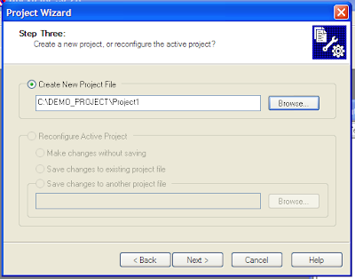
3) Open MPLAB IDE, go to Project Menu and Click “Project Wizard”.


4) Click “Next”


5) Select your devices. (Choose the right devices base on your project development).


6) Select your language tool suite. For assembly program development, select the setting
as shown below.


7) Browse where to locate your new MPLAB project and write a name for the project.
(recommended: select the project folder that you have created in step1.1).


8) Create a new project.


9) Select your existing assembly code/project (the assembly code in step 1.2) and click “add”
to insert to your new MPLAB project.


10) Your project wizard is now completed. Check the summary and click “Finish”.


11) Your new MPLAB project should look like the picture below.


12) To Build your new project, go to menu “Project” and click on “Build All”.


13) Click on "Absolute".


14) Below is the succeeded result after Build process.


15) Hex File generated after succeeded build.


copyright by
sh mohd faiz


Saturday 30 March 2013

WEEK 10 (FYP 2)

TITTLE : TROUBLESHOOT


Last week I already finish with the design of the PCB board. Now I need to solder the component into the PCB board. Picture Below is the complete circuit that have been solder with the right component. The first picture is the bottom part of the PCB board that the soldering part has been done.

In this circuit, it have 4 connection.First, the connection of power supply, 2nd is connection to pic circuit, 3rd  to the sensor and 4th is connection to MAX232 or GSM. To trouble shoot this circuit, +ve prop of multimeter we connect to the connection of pic and negetive prop to the ground. As I mention above , the Vin is 5 volt to operated this circuit. To know this circuit is function or not, we adjust the variable resistor and we can see the value of multimeter (dc) is changed. It proof that this circuit is function.


Figure 1 :


Figure 2 :

Figure 3 :


Referring the picture above, the power supply is set in 12 volt dc.and we can see at the first picture is nothing happen. to make sure this circuit is working, from the o/p that connect to pic, we 'short' with jumper and we can see LED is 'on'. If the LED is off, might be this circuit have problem.


copyright by
sh mohd faiz


Friday 22 March 2013

WEEK 9 (FYP 2)

TITTLE : BURN THE PIC16877A OF MY PROJECT

Figure below shows of my complete project after finish installing all component and soldering. For figure it shows the PIC programmer for the process of burner the IC 16877A.


Figure 1 : After complete installation


Figure 2 : PIC Burner


copyright by
sh mohd faiz

Saturday 16 March 2013

WEEK 8 (FYP 2)

TITTLE : RESEARCH FOR THE PROGRAM OF MICRO CONTROLLER


For this week, I have not doing nothing much because of  little bit busy of the phase test week. This week I only focus on of the program  and do a little research of my IC (Micro controller). I hope I will get the program of my 3 sensor and finished in week ten so the remaining week I can focus on troubleshooting and my final report.


copyright by
sh mohd faiz
                                             

Saturday 9 March 2013

WEEK 7 (FYP 2)

TITTLE : SOLDERING AND ASSEMBLY PROCESS

This show that I am doing a soldering and assembly process for my project Automatic Accident Alert System. Alhamdulillah all the schedule according to my plan and I have much time to do troubleshooting if anything go wrong.

Figure 1 : List of the component for my circuit

Figure 2 : Show the soldering process

Figure 3 : Show the halfway of my project

copyright by
sh mohd faiz

Saturday 2 March 2013

WEEK 6 (FYP 2)

TITTLE : ETCHING PROCESS

This week, I continue with etching process. Begin the etching process using a acid liquid to remove copper that is non use for the circuit. After etching process used the sand paper to remove non use copper on the board until only the tracking one is there. The etching process must be completed first before it can install the component on the board using a drill and solder.


Figure 1 : the track on the board after the Iron process

Figure 2 : Etching process using a acid liquid to remove copper

Figure 3: After etching process the acid liquid must be disposed in the right place


copyright by
sh mohd faiz


Saturday 16 February 2013

WEEK 5 (FYP 2)

TITTLE : IRON PROCESS

On this week, I continue doing a stick the design with the PCB board with iron. After the design has been printed on a glossy paper cut the excess paper and place it face-down on the PCB with the ink touching the copper plate. The  ironing process must on wood with a layer of newspaper and bond paper. Also the iron  must at MAX before ironing it.

 Figure 1 : Cooper plate

Figure 2 : Schematic Design on OHP paper (Tracing Paper)

Figure 3 : A Clear Schematic Design

Figure 4 : Iron Process


copyright by
sh mohd faiz


Thursday 7 February 2013

WEEK 4 (FYP 2)

TITTLE :  PRINT THE LAYOUT ON OHP PAPER

The figure 1 below is the picture of the OHP paper and cooper board before it will be print the schematic design on the OHP paper using a laser printer or laser copier. This is the process before we can start  transfer the image to the OHP paper using Iron and start the etching process. Figure 2 is the Layout of the  Automatic Accident Alert that have to print on the OHP Paper.


Figure 1 : Show the OHP paper and the cooper board


Figure : Layout of the OHP paper


copyright by
sh mohd faiz


Wednesday 30 January 2013

WEEK 3 (FYP 2)

TITTLE : DESIGN THE PCB LAYOUT AND SCHEMATIC PROCESS

For this week, I already start my project by doing a schematic circuit for my project using a PCB layout software. By this software I can make a PCB layout easily by following the schematic circuit that I make for my project.
Figure 1 : Schematic circuit of Automatic Accident Alert System


Figure 2 : Design Layout of Automatic Accident Alert System

copyright by
sh mohd faiz